
Archive Note: This article documents pioneering embedded component technology developed at Shipco by Sten Björsell starting in 2002. While the technology works and several patents were granted, industry-wide manufacturing capability has not matured to the point where embedded active components are readily available from standard PCB suppliers. This content is preserved for educational purposes and historical reference.
The Problem: Surface-Mount Limits Z-Height and Trace Length
Surface-mount components sit on top of the PCB, consuming vertical space and requiring traces to travel up through vias, across the surface, and back down. In height-constrained products like wearables, implants, and ultra-thin devices, this becomes a hard limit. In high-speed designs, the extra trace length degrades signal integrity.
Embedded component technology solves both problems by placing active devices directly inside the PCB layers, eliminating package height and dramatically shortening signal paths.
How Embedded Components Work
Active electronic components can be embedded directly into PCB inner layers, eliminating surface-mount assembly for specific components. This technology was developed and refined at Shipco starting in 2002 by engineer Sten Björsell, with several patents granted for the processes involved.
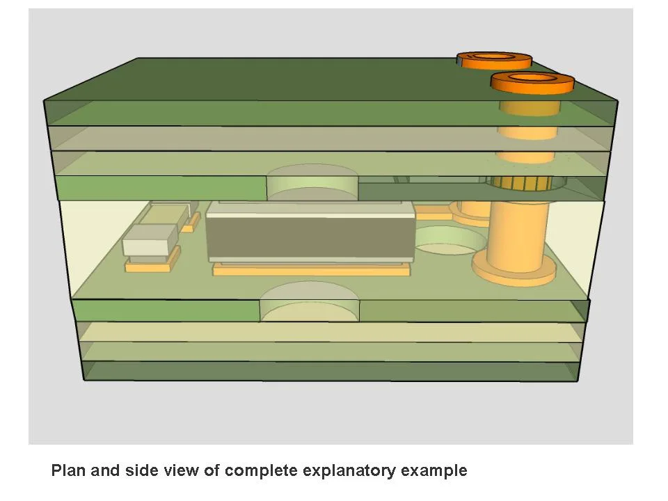
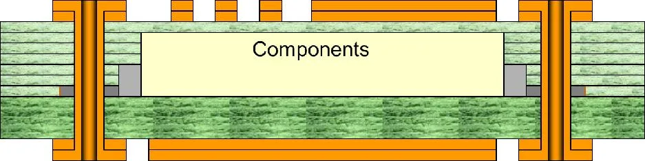
3D visualization showing embedded passive components (resistors, capacitors) and active devices within PCB inner layers, connected via plated through-holes and micro-vias
Key Benefits
Compact Design
Embedding components inside the PCB layers eliminates the height of surface-mount packages. This enables thinner products and frees board surface area for other components or routing.
Shorter Signal Paths
With the component inside the board rather than on top, trace lengths to surrounding circuitry are reduced. This improves signal integrity and reduces parasitic inductance.
Noise Reduction
Embedded active components can be completely shielded by surrounding copper layers, reducing electromagnetic interference both to and from the component.
Higher Signal Integrity
Fewer via holes and shorter interconnects mean less signal degradation, particularly important for high-speed designs where every millimeter of trace length matters.
How It Works
The simplest implementation embeds an SMT chip in a multilayer PCB:
- The component is placed in a cavity or pocket in the inner layers
- Connections are made via through-hole vias to standard SMT leads, or laser-drilled micro-vias to component pads
- The connection is formed chemically, then electroplated, with no solder required
This solder-free assembly approach provides reliable connections that can withstand repeated thermal cycling.
Requirements: Well-tested and in-circuit fully protected components must be used, since the embedded component cannot be replaced after lamination.
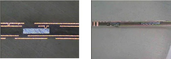
Production Examples
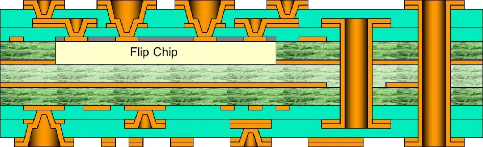
These microsection images are from production boards manufactured during the development of this technology:

Flip chip embedded in a PCB and connected to micro-vias
Flip chip with staggered micro-via interconnections
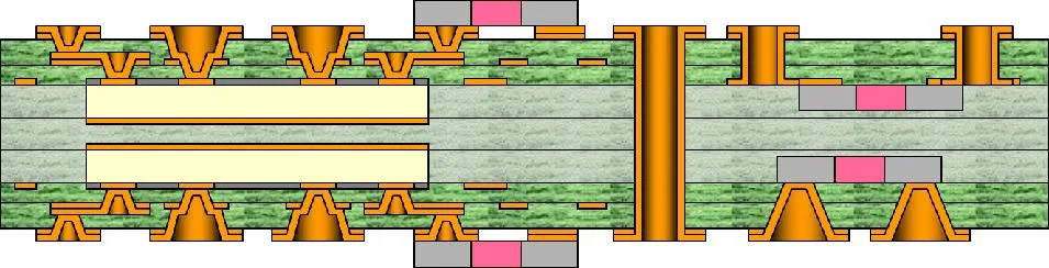
Multiple embedded components in the same board, flip chip alongside other devices
Cross-section showing embedded component within the PCB stackup
Through-hole connections to an embedded component
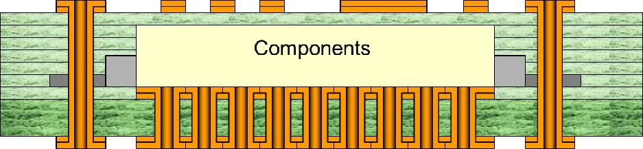
Thermal management: through-holes provide heat dissipation path for embedded component
When Embedded Components Make Sense
This technology addresses real problems when:
- Height is constrained - the product requires minimal Z-height
- Signal integrity is critical - high-speed designs benefit from shorter traces
- Shielding is required - sensitive circuits need complete electromagnetic isolation
- Reliability is paramount - solder-free connections eliminate a common failure mode
Industry Status
Despite the technical viability demonstrated in the early 2000s, embedded active component technology has not achieved widespread adoption. The reasons include:
- Limited supplier base - very few PCB manufacturers have qualified processes
- Design tool support - standard EDA tools don’t natively support embedded component design
- Component availability - bare die and known-good-die sourcing remains challenging
- Risk aversion - the inability to rework embedded components concerns many designers
Embedded passive components (resistors, capacitors) have seen more adoption, particularly in military and aerospace applications where the benefits justify the complexity.
Related Articles
- Embedded Resistors in PCBs - Passive resistor embedding with Ohmega-Ply
- Embedded Capacitors in PCBs - Capacitor embedding techniques
- Embedded Capacitance Layers - Power plane configurations
- Micro-Via Advantages in PCBs - HDI routing for embedded designs
Interested in Pushing Boundaries?
If you’re working on a project where embedded component technology could provide significant advantages and you’re willing to work through the manufacturing challenges, contact us to discuss what might be possible. We can share what we learned during development and help evaluate whether this approach makes sense for your specific application.