
Archive Note: Embedded capacitance layer technology using thin high-Dk dielectrics is technically viable, but supplier availability remains limited. Materials like DuPont Interra and 3M ECM exist, but finding PCB manufacturers with qualified processes requires effort. This article explains the technology for educational purposes.
The Problem: Decoupling Fails at High Frequencies
Discrete surface-mount capacitors work well for decoupling at moderate frequencies, but above 1 GHz they become ineffective. The culprit is parasitic inductance - the capacitor’s leads, solder joints, and PCB traces all add inductance that dominates at high frequencies, turning your decoupling capacitor into an inductor precisely when you need it most.
For high-speed digital designs, RF circuits, and power-integrity-critical applications, this creates a real problem: how do you provide low-impedance decoupling at frequencies where discrete components fail?
The Solution: Embed Capacitance in the Stackup
By forming capacitance directly within the PCB layer structure, you eliminate the parasitic inductance of discrete components entirely. A thin dielectric layer (typically 12 µm) sandwiched between copper planes creates distributed capacitance across the entire power plane area.
Key benefits:
- Effective decoupling above 1 GHz where discretes fail
- Minimal ESR and virtually zero lead inductance
- Reduced power bus noise and radiated emissions
- Smaller package size - fewer surface-mount components needed
- Built-in decoupling that doesn’t consume board space
A complete embedded capacitance stackup can be built below 0.35 mm thick, using three 50 µm prepreg layers, two 12 µm capacitance dielectrics, and 18 µm copper foil.
Dielectric Material Options
DuPont and 3M both offer high-capacitance dielectric laminates designed for this application:
Example Stackup: Embedded Capacitance with Blind Vias
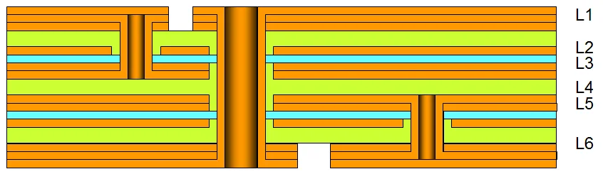
Multilayer stackup with embedded capacitance layers accessed through blind vias
This configuration uses blind vias to connect surface components directly to the embedded capacitance planes, minimising the inductance path.
Layer Composition
| Layer | Thickness |
|---|---|
| Final plating | 18 µm |
| Second plating | 18 µm |
| Base copper | 18 µm |
| Core | 100 µm |
| Base copper | 18 µm |
| Capacitance layer | 12 µm |
| Base copper | 18 µm |
| Second plating | 18 µm |
| Prepreg | 100 µm |
| Second plating | 18 µm |
| Base copper | 18 µm |
| Capacitance layer | 12 µm |
| Base copper | 18 µm |
| Core | 100 µm |
| Base copper | 18 µm |
| Second plating | 18 µm |
| Final plating | 18 µm |
Total thickness: 0.44 mm
Example Stackup: Embedded Capacitance Without Blind Vias
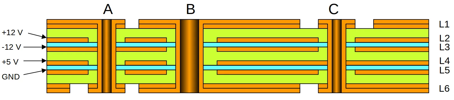
Simpler stackup using embedded capacitance as distributed power planes
This approach treats the capacitance layers as distributed power planes rather than point connections. In the example shown:
- Plane A connects to −12 V
- Plane C connects to +5 V
- Plane B is isolated (signal reference or unused)
Layer Composition
| Layer | Thickness |
|---|---|
| Final plating | 18 µm |
| Base copper | 18 µm |
| Core | 100 µm |
| Base copper | 18 µm |
| Capacitance layer | 12 µm |
| Base copper | 18 µm |
| Prepreg | 100 µm |
| Base copper | 18 µm |
| Capacitance layer | 12 µm |
| Base copper | 18 µm |
| Core | 100 µm |
| Base copper | 18 µm |
| Final plating | 18 µm |
Total thickness: 0.368 mm
When to Consider Embedded Capacitance
This technology addresses real problems when:
- Your design operates above 500 MHz and discrete decoupling isn’t cutting it
- Power integrity analysis shows impedance problems in the GHz range
- Board space is constrained and you need to reduce component count
- EMI/EMC compliance is challenging due to power bus noise
Industry Status
Embedded capacitance layer technology requires specialized materials and fabrication processes that are not universally available. The challenges include:
- Material sourcing - high-Dk thin dielectrics are specialty products
- Process qualification - handling ultra-thin layers requires specific equipment and expertise
- Lead times - expect longer procurement cycles for non-standard materials
- Cost - premium over standard FR-4 stackups
This technology sees use in high-reliability applications (aerospace, defense, medical) where the performance benefits justify the complexity and cost.
Related Articles
- Embedded Capacitors in PCBs - Discrete capacitor embedding techniques
- Embedded Components Overview - Active component embedding technology
- PCB Materials and Laminates Guide - Dielectric material specifications
Questions?
If you’re evaluating embedded capacitance layers for a specific application, contact us. We can discuss the technology and help you understand whether it makes sense for your requirements.