
via
Plated hole connecting traces between PCB layers.
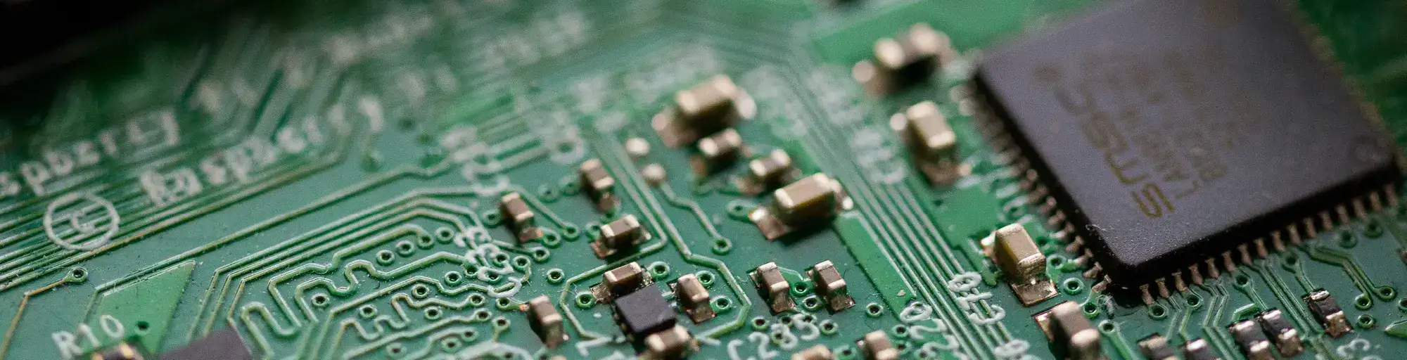
Definition
A via (vertical interconnect access) is a plated hole that electrically connects traces on different PCB layers. Through-vias span the entire board thickness; blind vias connect an outer layer to inner layers; buried vias connect only inner layers. Via size affects routing density and signal integrity - smaller vias allow tighter routing but cost more. Standard vias are 0.3mm drill/0.6mm pad; micro-vias are ≤0.15mm laser-drilled. Via placement affects impedance (stubs), thermal performance (thermal vias), and HDI capability.