
copper plating
Electrochemical deposition of copper to build up trace thickness and plate hole walls.
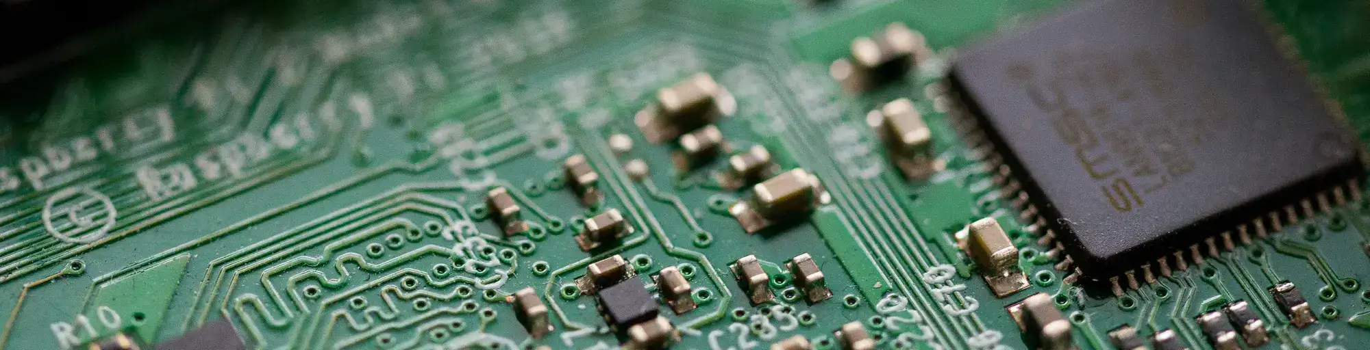
Definition
Copper plating deposits copper onto PCB surfaces through electrochemical reduction. Two types: electroless (chemical reduction, provides initial conductivity on drilled hole walls) and electrolytic (uses applied current, builds up thickness). Standard process adds 20-25µm to hole walls; thicker plating improves reliability but reduces hole diameter. Plating distribution depends on pattern density - isolated features plate thicker than dense areas. Plating thickness affects impedance (thicker traces have lower impedance), current capacity, and via reliability. Quality is verified through microsection measurement.